Semiconductors are considered the brains of modern electronics. Our TIGER OPTICS™ Cavity Ring-Down Spectroscopy (CRDS) gas analyzers seamlessly detect parts-per-billion (ppb) and parts-per-trillion (ppt) levels and delivers bulk gas monitoring for trace H2, H2O, O2, CH4, CO, CO2, Kr, NH3, and Xe, UHP ammonia for HB LED production, tool monitoring for trace H2O and HF, and continuous AMC monitoring for ambient HCl, HF, and NH3.
Specialty gases of superior quality play a vital role as raw materials and process gases across various industries. From carbon dioxide in beverages to ammonia in LED manufacturing and silane in semiconductor fabrication, maintaining high purity standards for specialty gases is critical. The presence of moisture impurities, for instance, can significantly impact the efficiency of resulting LEDs. The semiconductor industry demands ultra-high purity gases, whether it’s silane or germane for epitaxy, fluorine compounds for etching processes, or cleaning gases. Process Insights offers highly sensitive, accurate, and user-friendly analysis instruments. These instruments utilize the renowned Cavity Ring-Down Spectroscopy (CRDS) technique and cater to a wide range of specialty gases and applications.
What is Cavity Ring Down Spectroscopy?
Technical Specifications of Tiger Optics CRDS
Cavity Ring-Down Spectroscopy: Principles, Applications, and Benefits
Trace Moisture Analysis with CRDS
What is a trace moisture analyzer
The Purity Imperative: Specialty Gases for Critical Industries
-
Beverages
-
LED manufacturing
-
Semiconductor fabrication
- Medical and pharmaceutical applications
-
Aerospace and defense
- Benzotriazole Monitoring in Semiconductors with Fiber Optic UV-Vis Spectroscopy
The High-Stakes Reality of Impurities
-
Moisture contamination can reduce LED brightness and lifespan
-
Oxygen impurities can damage semiconductor wafers
-
Carbon dioxide purity affects beverage taste and shelf life
Ultra-High Purity Demands
-
Silane and germane for epitaxy processes
-
Fluorine compounds for etching
-
Cleaning gases for contamination control
-
Nitrogen and argon for chamber purging


SALES | TRAINING INQUIRIES
AMERICAS: info.americas@process-insights.com
EMEAI (includes India): info.emeai@process-insights.com
APAC: info.apac@process-insights.com
CHINA: info.cn@process-insights.com

NIR Optical Analyzers for Liquids and Gases
From dynamic chemical blending and wafer cleaning to metals concentration monitoring and on-site gas blending, precision matters.
✅ In situ monitoring improves yields, reduces chemical waste/costs, and optimizes cycle times.
✅ Detect metals contamination down to 5 ppm with GUIDED WAVE 508 UV-VIS and Clearview db.
✅ Ensure stable, on-demand gas blends with real-time NIR quality data.
With our GUIDED WAVE Clearview db product line, you get 24/7 critical process data to keep operations running at peak performance.

Cavity Ring-Down Spectroscopy (CRDS) gas analyzers from Process Insights have a long history in industrial gas, medical gas, and chemical processing, enabling the detection of moisture and other rogue impurities in process gas streams, including inert, reactive, corrosive, bulk, and specialty gases.
Cavity Ring-Down Spectroscopy (CRDS) Technology delivers a highly sensitive and precise analytical technique used for the detection and measurement of trace gases and isotopes in a sample. It is a non-destructive technique that provides quantitative measurements of molecular absorption spectra.


T-I MAX X3 Airborne Molecular Contaminant (AMC) MONITORING SOLUTION
Simultaneously Monitor HF, HCl, and NH3 in Real-Time – Next-Generation Trace Gas Analyzers for Detection & Continuous Monitoring of Airborne Molecular Contaminants in Semiconductor Cleanrooms, FOUP Cleaning Tools, Reticle Nests and Sub Fab Environments. Our T-I Max™ series analyzers monitor invisible defect generators, commonly found lurking in and around equipment, personnel, wafer carriers and cleanroom bays.


MAX300-TGM™ TOXIC GAS MONITOR
Our EXTREL™ MAX300-TGM™ Toxic Gas Monitor is a real time monitoring solution with analysis speeds of 0.4 seconds per chemical and gas clearing times of less than 3 seconds. These impressive speeds exceed industry requirements for continuous monitoring. With the ability to analyze 15+ chemicals per sample point, the MAX300-TGM toxic gas analyzer provides maximum efficiency at an extremely low cost-per-chemical, per sample point.


VeraSpec™ APIMS™
Our TIGER OPTICS™ VeraSpec™ Atmospheric Pressure Ionization Mass Spectrometer (APIMS) is designed for reliable and repeatable low parts-per-trillion detection limits for contamination control in Ultra-High Purity (UHP) gases used in semiconductor and other high-tech industrial applications.
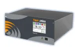
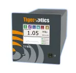
Tiger Optics UHP gas analyzers WITH crds tECHNOLOGY
CQC / IQC Cabinet Total Monitoring Solution

VeraSpec™ APIMS

GO-cart™ for AMC Monitoring

GO-cart™ for Analytical Monitoring

HALO Max QCL™ CO2

HALO Max QCL™ CO
HALO KA™ H2O

HALO KA Max™ CH4

HALO KA Max™ H2O

HALO KA Max™ NH3

T-I Max EtO™

HALO™ 3 CH2O

HALO™ 3 CO

HALO™ 3 CO2
HALO™ 3 D2O/HDO

HALO™ 3 H2O

HALO™ 3 CH4

HALO™ 3 HCl

HALO™ 3 NH3

HALO 3 HF

HALO™ H2
HALO™ H2O in N2O

HALO™ OK/OK+

HALO™ LP H2O

HALO™ RP

HALO™ QRP
Spark™ H2O

Spark™ H2O in CO2

Spark™ CH4

Spark™ C2H2

Spark™ CO2

Spark+™ CO

Spark Max™ CO2

Prismatic 3™

Prismatic 3+™
T-I MAX™ AIR GHG

T-I MAX X3

T-I MAX™ HCl

T-I MAX™ HF

T-I MAX™ NH3
T-I MAX™ CEM

CO-REKT™

ALOHA+H2O™
